The Belgian Microelectronics Research Center (imec) has joined hands with AIXTRON, GlobalFoundries, KLA, Synopsys and Veeco to become the first research partners in its 12-inch gallium nitride (GaN) open innovation research direction, targeting the...
The Belgian Microelectronics Research Center (imec) has joined hands with AIXTRON, GlobalFoundries, KLA, Synopsys and Veeco to become the first research partners in its 12-inch gallium nitride (GaN) open innovation research direction, targeting the application of low-voltage and high-voltage power electronic components.
Imec pointed out that the research direction with its partners is part of the imec Gallium Nitride Power Component Industry Alliance Program (IIAP), which is established to develop 12-inch gallium nitride epitaxial growth and high-voltage and low-voltage gallium nitride high electron mobility transistor (HEMT) process flows. The use of 12-inch substrates will not only reduce the manufacturing cost of gallium nitride components, but also enable the development of more advanced power electronic components in the future, such as high-efficiency low-voltage point-of-load (POL) converters for CPUs and GPUs.
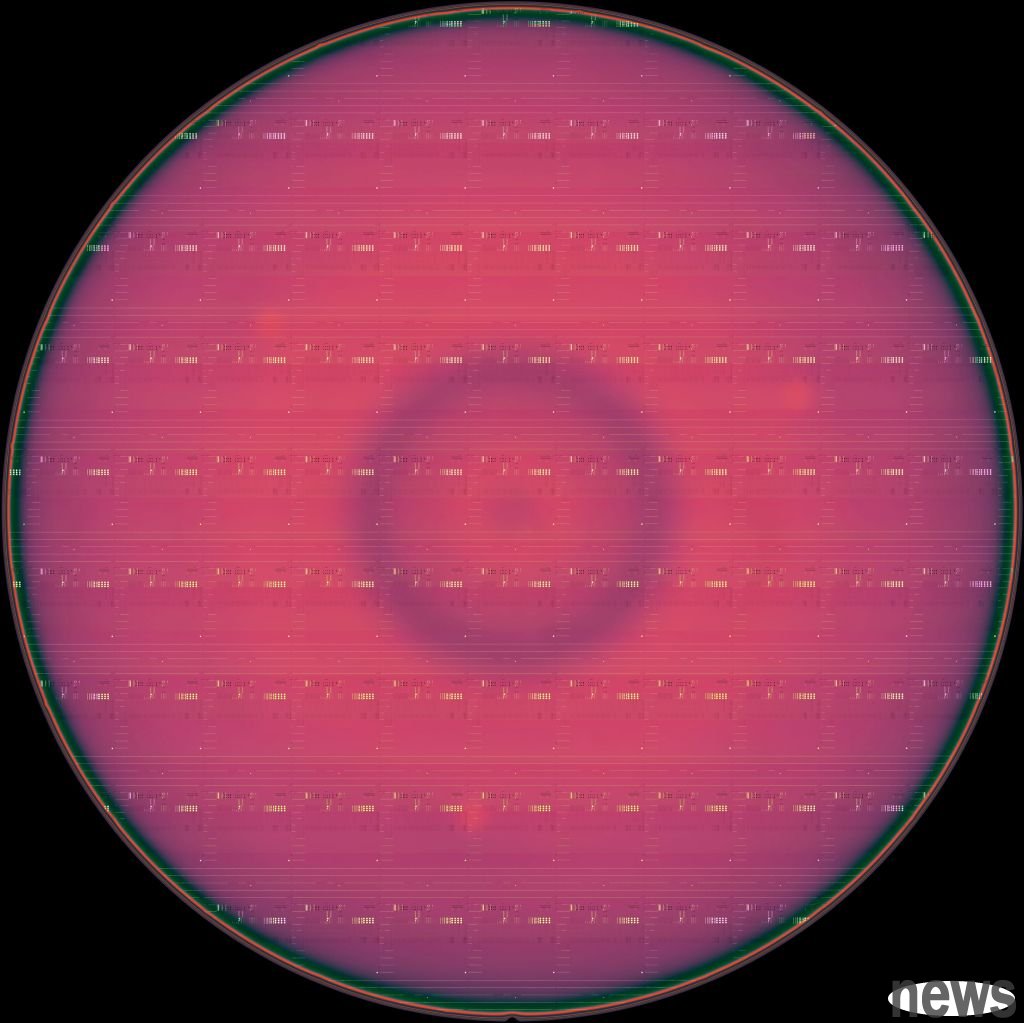 ▲ The 12-inch gallium nitride on silicon wafer supplied by AIXTRON was inspected on the 8 series/CIRCL tool provided by KLA after imec completed the p-type gallium nitride etching.
The market demand for gallium nitride fast chargers has increased, which highlights the development potential of gallium nitride technology in power electronic applications. Backed by continued advances in gallium nitride epitaxial growth, gallium nitride component and wafer manufacturing, reliability and robustness, and system-level optimization, gallium nitride technology is ready to enable a new generation of power electronics. When these products enter the market in the future, they will have smaller size, lighter weight and better energy conversion efficiency than silicon-based solutions. For example, on-board chargers and DC/DC converters for automotive applications, inverters for solar panels, and power distribution systems for telecommunications and AI data centers—GaN-based components are used in these applications to provide comprehensive decarbonization, electrification, and digitalization of society.
A clear trend in GaN technology development is the shift to larger wafer sizes, with most available capacity currently being 8 inches. As imec proposes the research direction of 12-inch gallium nitride, imec is currently taking the next step based on its 8-inch wafer expertise. Stefaan Decoutere, Imec technical academician and director of the gallium nitride power electronics research project, said that the benefits of switching to 12-inch wafers go beyond increasing production scale and reducing manufacturing costs. The CMOS-compatible GaN technology we developed is now available in leading 12-inch devices, which will allow us to develop more advanced GaN power devices. For example, ultra-miniature low-voltage p-type gallium nitride gate HEMTs for POL converters enable energy-efficient power distribution for CPU and GPU applications.
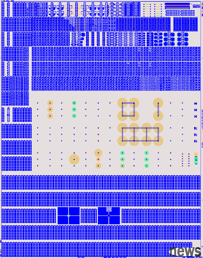 ▲ Mask set for the development of gallium nitride (GaN) high electron mobility transistors (HEMT) using 12-inch substrates.
As part of the 12-inch gallium nitride research plan, a baseline lateral p-type gallium nitride HEMT technology platform will be established in the future to target low-voltage applications such as 100V, using 12-inch silicon (111) material as the substrate. To this end, process modules based on p-type gallium nitride etching and ohmic contact forming are currently being studied. Then came the focus on high-voltage applications. For applications above 650V, development will use a 12-inch SEMI-compliant, CMOS-compatible QST substrate (material containing a polycrystalline aluminum nitride core layer). During these development stages, controlling the curvature of the 12-inch wafer and its mechanical strength are major considerations.
The launch of the 12-inch gallium nitride research project follows the successful completion of the 12-inch wafer loading test and mask set development. Imec expects to have all 12-inch wafer capacity set up in its 12-inch clean rooms by the end of 2025. Stefaan Decoutere emphasized that the success of 12-inch GaN development also relies on the ability to establish a robust ecosystem and jointly drive innovation, including 12-inch GaN growth and process integration to packaging solutions. Therefore, we are pleased to announce that Aixtron, GlobalFoundries, AmeriCorps, Synopsys and Welter Instruments have become the first batch of research partners in our 12-inch gallium nitride open R&D research direction, and we hope to welcome more partners in the near future. Because developing advanced GaN power electronics requires a close connection between design, epitaxy, process integration and applications—a connection that has proven critical in our forward-looking research on 8-inch GaN.